


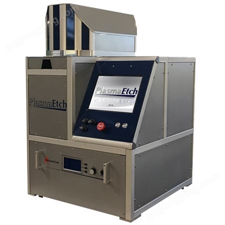
CuProtect工艺 - 美国8,945,343 B2-用施加的电压解封装。 具有铜线防护的化学芯片开封系统 ---- JetEtch Pro CuProtect Protecting Those Sensitive Copper Wires.
| |
It got easier.With the price of gold at an all-time high, a current trend in the manufacturing of integrated circuits is the shift from gold to copper bond wires. With this shift, the failure analyst of these processors is now challenged to successfully attain package decapsulation by use of traditional methods.
主要特征(Features):Patented Bias Technology Advanced Software Affordable All JetEtch Pro Features |  |
The Old Methods.Historically, one would use an automated chemical decapsulation system to etch samples with copper wires — with minimal success. Even with a low-temperature nitric and sulfuric acid mixture, and even in combination with laser pre-opening, this process works to an extent, but is largely unreliable. When faced with a limited number of field failures, which is a common scenario in a failure analysis laboratory setting, less reliable processes can’t be counted on to deliver satisfactory failure analysis and visual inspection results. The Solution.To support manufacturers in making this shift so that failure analysis can still be performed on their most advanced and cutting edge products which now use copper wire bonding, Nisene Technology Group has developed a version of its new JetEtch Pro decapsulation system that is specifically designed to handle the processing of this sensitive material: the JetEtch Pro CuProtect — the latest in a series of innovative solutions for the failure analysis industry from Nisene. | |
The Process.Using a proprietary and patented process, the JetEtch Pro CuProtect applies a bias to the solution being pumped to the sample in the process chamber. This bias creates a condition in which negatively-charged sulfate ions are attracted and temporarily bond to the surface of the copper wire while the sample is being etched. This temporary sulfate ion coating protects the copper wires from corrosion while the sample undergoes the etching process. The image to the right illustrates the operating principal behind the technique. Click on the image to open a larger version in a new window. In less sophisticated systems relying solely on low temperature etching, positively-charged hydrogen ions are attracted to the copper wires, thereby making the wires susceptible to pitting, cracking, breaking, and many other undesirable anomalous artifacts that greatly affect or even squelch completely the ability to perform failure analysis after the etching process. The Nisene Technology Group CuProtect system solves this problem. | |
The Results.As illustrated in the images below, the advanced bias application process yields results that are unmatched in the industry. If you would like to see more examples of samples etched with the CuProtect, please contact us. The Software.“Surely something like this must be complicated to use and difficult to understand — right?" you ask. The answer to that is “of course not!" The system appears on the outside to be the same as the JetEtch Pro, but there is an added line in its decapsulation programming menu that allows the user to change the value of the applied bias. The range is 0 V (off or no bias) to V, selectable in .1 V increments. The other differences between the CuProtect system and the JetEtch Pro — both in hardware and software — are hidden inside the system, so operating the CuProtect is exactly like JetEtch Pro and virtually transparent to a user. That is to say: learning curve is very small. There’s no need to learn anything new other than how much voltage to apply to your sample while it is etching.
One additional parameter line. Not much to learn here! | |


所有评论仅代表网友意见,与本站立场无关。